
 中文
中文
 English

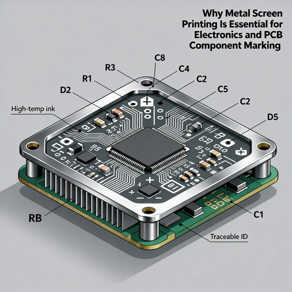
Why Metal Screen Printing Is Essential for Electronics and PCB Component Marking
In modern electronics manufacturing—particularly for power electronics, automotive systems, and industrial control units—increasing reliance on metal-clad printed circuit boards (PCBs), copper- or aluminum-based heat-sink assemblies, and hybrid substrates has introduced unique challenges in component marking. Conventional solder mask–based labeling methods often fail under thermal cycling, mechanical abrasion, or prolonged exposure to high-temperature reflow processes. Metal screen printing has emerged as a robust, scalable, and standards-compliant solution for permanent, high-fidelity marking directly onto metal substrates.
Unlike traditional silkscreen printing on FR-4 laminates, metal screen printing employs specially formulated inks engineered for adhesion to bare or anodized metals—including aluminum, stainless steel, copper, and nickel-plated surfaces. These inks are typically ceramic-loaded or epoxy-acrylic hybrids, delivering exceptional resistance to temperatures exceeding 300 °C—making them compatible with lead-free reflow profiles, wave soldering, and post-assembly cleaning chemistries. This capability positions metal screen printing as a critical enabler of traceability, functional annotation, and regulatory compliance in mission-critical applications.
One of the most significant advantages lies in its role as a viable solder mask alternative for metal-based PCBs. Where conventional solder masks cannot bond reliably to non-dielectric substrates—or degrade under thermal stress—metal screen printing provides precise, durable definition of solder pads, fiducial markers, polarity indicators (e.g., “+”, “−”, or cathode notches), and reference designators. The process achieves line widths down to 150 µm with registration accuracy within ±25 µm, supporting miniaturized layouts without compromising legibility or process repeatability.
Moreover, component identification on metal substrates benefits directly from the chemical and mechanical stability of high-temperature resistant ink systems. Printed markings retain contrast, dimensional integrity, and barcode/QR code scannability after multiple thermal cycles, vibration testing, and exposure to conformal coatings or potting compounds. This ensures unambiguous part-level traceability throughout product lifecycle—from assembly and test through field service and end-of-life recycling—meeting IPC-A-610, IPC-J-STD-020, and ISO/IEC 15415 requirements.
From a production standpoint, metal screen printing integrates seamlessly into existing SMT lines. It supports both manual and automated screen printing platforms, requires no substrate pre-treatment beyond standard cleaning, and offers rapid changeover between job families. Compared to laser marking—which may induce micro-cracking or alter surface conductivity—screen printing adds negligible mass, maintains electrical insulation where required, and avoids localized thermal stress that could compromise adjacent components or metallization layers.
As electronics continue shifting toward higher power density, wider bandgap semiconductors (e.g., SiC and GaN), and embedded passive integration, the demand for reliable, high-performance marking solutions on metal substrates will only intensify. Metal screen printing electronics is no longer a niche option—it is an essential process for ensuring manufacturability, quality assurance, and long-term reliability in next-generation electronic assemblies.